
- Optical Transceivers
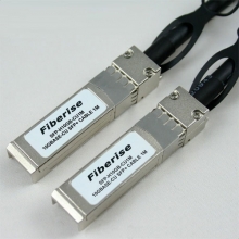
- SFP+ Transceivers
- XENPAK Transceivers
- XFP Transceivers
- X2 Transceivers
- SFP Transceivers
- Compatible SFP
- 3Com SFP
- Alcatel-Lucent SFP
- Allied Telesis SFP
- Avaya SFP
- Brocade SFP
- Cisco SFP
- D-Link SFP
- Dell SFP
- Enterasys SFP
- Extreme SFP
- Force10 SFP
- Foundry SFP
- H3C SFP
- HP SFP
- Huawei SFP
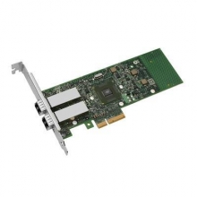
- Intel SFP
- Juniper SFP
- Linksys SFP
- Marconi SFP
- McAfee SFP
- Netgear SFP
- Nortel SFP
- Planet SFP
- Q-logic SFP
- Redback SFP
- SMC SFP
- SUN SFP
- TRENDnet SFP
- ZYXEL SFP
- Other SFP
- FE SFP
- GE SFP
- OC3 SFP
- OC12 SFP
- OC48 SFP
- Copper SFP
- CWDM SFP
- DWDM SFP
- BIDI SFP
- Fiber Channel SFP
- Multi-Rate SFP
- SGMII SFP
- Compatible SFP
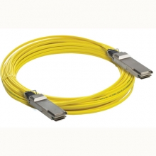
- GBIC Transceivers
- Passive Components
- Networking
- Cables
- Equipments
- Tools
- Special Offers
Brands

Industry News

Fiber Optic Wiki

Description Of Photonic Crystal
Photonic crystals are periodic optical nanostructures that are designed to affect the motion of photons in a similar way that periodicity of a semiconductor crystal affects the motion of electrons. Photonic crystals occur in nature and in various forms have been studied scientifically for the last 100 years.
Photonic crystals are composed of periodic dielectric or metallo-dielectric nanostructures that affect the propagation of electromagnetic waves (EM) in the same way as the periodic potential in a semiconductor crystal affects the electron motion by defining allowed and forbidden electronic energy bands. Essentially, photonic crystals contain regularly repeating internal regions of high and low dielectric constant.
Photons (behaving as waves) propagate through this structure - or not - depending on their wavelength. Wavelengths of light that are allowed to travel are known as modes, and groups of allowed modes form bands. Disallowed bands of wavelengths are called photonic band gaps. This gives rise to distinct optical phenomena such as inhibition of spontaneous emission, high-reflecting omni-directional mirrors and low-loss-waveguiding, amongst others.
Since the basic physical phenomenon is based on diffraction, the periodicity of the photonic crystal structure has to be of the same length-scale as half the wavelength of the EM waves i.e. ~350 nm (blue) to 700 nm (red) for photonic crystals operating in the visible part of the spectrum - the repeating regions of high and low dielectric constants have to be of this dimension. This makes the fabrication of optical photonic crystals cumbersome and complex.
November 7, 2011
Featured


Bestsellers


Registered Names and Trademarks are the copyright and property of their respective owners.
Copyright © 2026 Fiberise(A company of Cablexa Ltd). All rights reserved.
Copyright © 2026 Fiberise(A company of Cablexa Ltd). All rights reserved.